MEMS Foundry
Innovation Engineering operates a state-of-the-art 2650 m2 pure-play MEMS Foundry on the High Tech Campus in Eindhoven, the Netherlands. This MEMS Foundry is specialized in low to medium volume custom MEMS manufacturing. When off-the-shelf components do not meet your requirements, and you consider having a custom MEMS device especially made for you, you come to us.
About our pure-play MEMS Foundry
We’ve been around for over 40 years. We’re born out of Philips Research and have matured into a pure-play MEMS Foundry. We now work for a wide range of technology leaders, mainly medium to large and growing high-tech enterprises. What our customers value about our pure-play MEMS Foundry is our responsiveness to change requests, and our ability to provide creative out-of-the-box solutions for the ‘seemingly impossible’. We are certified for:
ISO 9001:2015 ISO 14001:2015 ISO 13485:2016
MEMS wafer types
MEMS manufacturing of 4, 6, 8 inch and even square substrates. The MEMS Foundry offers the flexibility to use substrate materials like silicon, SOI, GaAs, glass, quartz and CMOS-wafers. At the foundry we offer services with high quality and reliability: advanced process development, prototyping, and low to medium volume manufacturing.
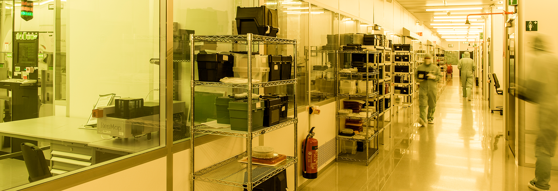
An impression of our 2650m2 MEMS Foundry
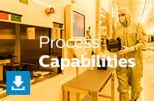
MEMS Foundry process capabilities
- We deliver more than 15,000 wafers per year from our ISO 5, 6 and 7 class cleanroom (equivalent to 100 – 10,000 FED standard class)
- We offer the flexibility to work with materials ranging from Ag to Zn, including ‘CMOS-forbidden’ materials, alloys, dielectrics and polymers like parylene.
Download the full specifications list on our process capabilities ›
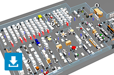
MEMS Foundry floorplan
Take a look at the floorplan of our 2650 m2 pure-play MEMS Foundry to see the layout of wet processing, lithography, deposition & plasma etching, furnaces, metrology, grinding & back-end processing areas.
A practical guide to select a MEMS partner
Choosing the right MEMS partner to suit your specific needs can be a challenge.
To help you make the right choice, we have indentified 8 key selection criteria which can act as your guide through the MEMS marketplace.
- How to prepare yourself for a MEMS project
- What to expect when starting a MEMS project
- Top 8 selection criteria to ask your potential MEMS partner
- A practical guide to define your requirements
- MEMS partner types – find the partner that fits best for you
- Additional information on how to make the guide work for you
Why work with our pure-play MEMS Foundry?
- The flexibility in working together
- Our responsiveness to change requests
- Our ability to provide creative out-of-the-box solutions for the ‘seemingly impossible’ – a capability developed from working with Philips Research for over 40 years
- Manufacturing MEMS devices under ISO 13485 and 9001
- 2650 m2 state-of-the-art cleanroom of class 100 – 10,000 (ISO class 5-7)
- Flexibility to work with materials ranging from Ag to Zn, including ‘CMOS-forbidden’ materials, alloys, dielectrics and polymers like parylene
- Flexibility to work with Si, III/V, GaAs, glass, quartz, square and round substrates, up to 8”
How we handle your MEMS Foundry project
Our process is designed to ensure confidentiality and secure your satisfaction on the required outcome, right from the start.
Needs assessment phase
After your request for information, we talk about what you want and need. We also discuss what we can do and deliver. Typically a non-disclosure agreement (NDA) will be signed to enable the exchange of confidential information. Then we will have calls, visits and in-depth technical discussions involving our experts, who have high levels of seniority and experience. In this way we get to know each other and establish whether we are a good match. A project proposal and a formal quotation with terms and conditions (GTC) complete this phase.
Project phase
With these MEMS Foundry services we cover the design, development and delivery phases of a MEMS project. Starting with your formal ‘go’, we run a phase-gated process development project, with the following three main phases:

In the early stages we deliver a preliminary MEMS manufacturing process flow. Further staps are taken to determine manufacturability of the MEMS device, followed by the implementation of the MEMS Foundry process flow, functional samples and most likely some iterations. This will get us to a MEMS proof of concept.

Your MEMS proof of concept needs to be further developed into a device that is ready for manufacturing with constant quality and yield. So the next step is to develop a MEMS manufacturing process flow. At the MEMS Foundry we develop a process flow ready for manufacturing, and provide you with devices for verification of its functionality and quality.

We manufacture your devices according to your specifications. Your annual order volumes may range from 10 to 5,000 wafers. Statistical process control are standard. Multiple production runs are used to iron out any significant quality or yield issues, resulting in a MEMS manufacturing process delivering high quality, repeatability and reliability.
Key application areas
New digital printing application areas, breakthrough technology & cost advantage with custom thin-film MEMS inkjet printheads.
Manufacturing of devices like meshes, nozzles, jets, channels, barriers and complete functional chips.
Breakthrough applications for ultrasound, complementing conventional technology with advantages.
Benefit from unique BioMEMS expertise that has helped leading BioMEMS companies successfully turn their imaginative ideas into working devices.
