Microfluidic Devices
When developing a microfluidic device, there are many factors to consider: channel designs and sizes, control over critical dimensions, layer alignment, which type of materials or lithography processes can be used, etc.
Think of what an experienced partner can do for you, imagine your development further down the road. Don’t you want a flexible development and reliable manufacturing company to ensure your device is brought to volume and to market quickly?
Our experts are here to think along with you and accelerate your innovation with clever approaches in designing and manufacturing. We have been working on microfluidic technology for over 15 years now, and we are ready to share our knowledge with you.
How can we help you with your microfluidic device?

Elena Beletkaia
Business Development Manager
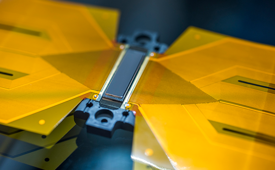
MEMS for Microfluidic Devices
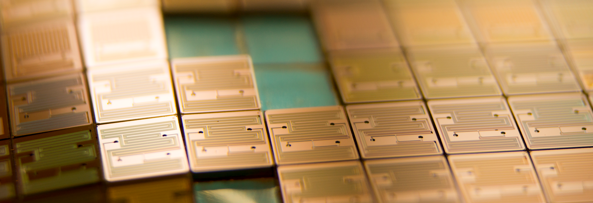
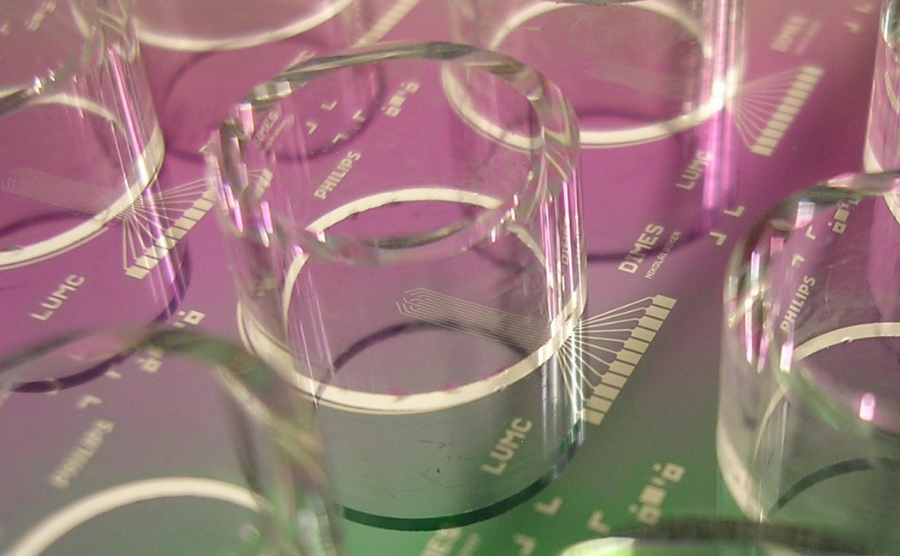
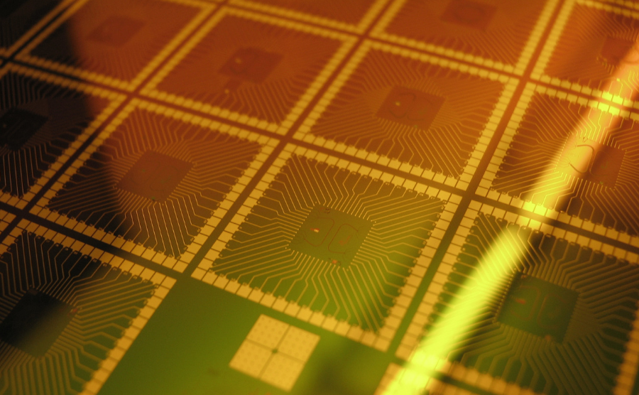
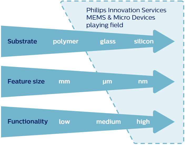 Micro-Electro Mechanical System (MEMS) are mechanical and electrical structures in silicon wafers using photolithography, etching and deposition processes to create structures for microfluidics. Using MEMS & thin film technologies like lithography, nano-imprint, dry and wet-etching, deposition, and a variety of laser systems, we can manufacture microfluidic devices in a range of substrate materials like silicon, glass, polymers or metal.
Examples of microfluidic applications:
- Wells
- Nozzles
- Jets
- Channels
- Barriers
- Complete functional chips
Flexibility in substrates & materials
A wide range of choice in biocompatible materials:
- Polymers
- Metals
- Oxides
- Application tailored solutions
Choice in deposition techniques to suit your application:
- Evaporation
- Sputtering
- Chemical vapor deposition
- Spin coating
- Spray coating
- Atomic layer deposition
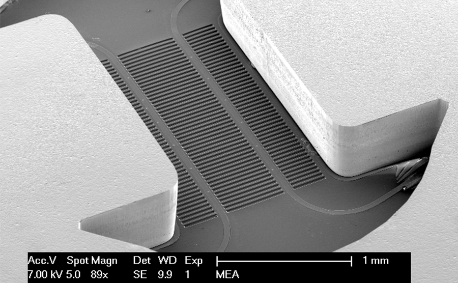
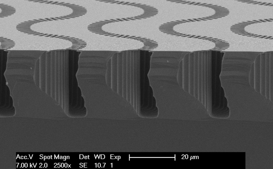
Feature size
MEMS giving high functionality to microfluidics
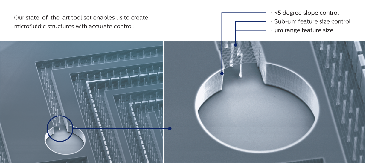
In the spotlight: manufacturing µF structures with laser

Presentation by technologist René Sanders, at the Polymer Replication on Nanoscale conference, on the standardization and manufacturability of microfluidic structures using the laser method. Read article ›

What sets us apart?
- Device design – combining customer’s application know-how and our own experience
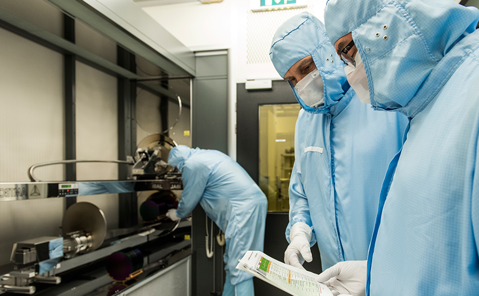
- Process development – state-of-the-art MEMS fabrication equipment, experienced engineering crew
- One-stop-shop – from device and process concept development to volume manufacturing, integration of electronics, and assembly services
- Pure-play MEMS foundry – for over 30 years we have been working for industry leaders with high confidentiality and IP protection demands
- High customer satisfaction – NPS score +50%
MEMS Foundry services
MEMS Foundry services involved in the manufacturing of microfluidic devices.
Relevant for you: MEMS & Micro Devices
We are Philips Engineering Solutions and we operate a state-of-the-art 2,650 m² pure-play MEMS foundry in Eindhoven, the Netherlands. We offer in-house MEMS & Micro Devices services. At the MEMS Foundry and Micro Devices Facility we offer advanced prototyping, development and volume manufacturing services for MEMS microfluidics devices, both for components and for complete module assemblies. Our MEMS technology enables high volume manufacturing and high levels of integration at a lower cost. You benefit from our expertise, built from developing and manufacturing a range of microfluidics devices. Our MEMS technology platform shortens design cycles and therefore your time-to-market. Partnering with Philips Engineering Solutions is the quickest way to obtain a reliable MEMS microfluidic chips. Sustainable competitive advantage through custom MEMS devices. Check out our services in the MEMS & Micro Devices key area of expertise.