
‘There is more than Moore’; the catchphrase that planted the seed for Philips MEMS Foundry
To our engineering teams, the words ‘it cannot be done’ work like a magic charm. They take pride in solving the seemingly impossible. In the interview series ‘Our eureka moment’, engineers talk about these breakthroughs; what challenges did they face and how did they overcome them, together with their colleagues?
Moore’s Law is so famous, that even outside the semiconductor industry, many people know what it means: the number of transistors on microchips is expected to double every two years. The theory illustrates how mind-blowingly fast semiconductor technology develops.
About twenty years ago, a courageous research group at Philips took the plunge to challenge their leaders to look beyond Moore’s Law. Philips should not just focus on making microchips faster and smaller, they plead, but also look at how semiconductor technology can be used to develop a whole new area of micro devices and systems.
They succeeded. In fact, the idea that ‘there is more than Moore’ was followed by a series of events that eventually led to the Philips MEMS Foundry as we now know it.
On the verge of standard silicon processing and MEMS
Gerjan van de Walle, who currently works as a Business Partner in Engineering Solutions, was the group leader of Integrated Device Technologies in 2003. “We already performed research on several microsystem technologies; from biosensors to trench capacitors and fluidic manipulations. You can say that we were operating at the verge of standard silicon processing and MEMS.”
“In 2003, we already performed research on several microsystem technologies; from biosensors to trench capacitors and fluidic manipulations. You can say that we were operating at the verge of standard silicon processing and MEMS.”
Gerjan van de Walle, Business Partner
Gerjan: “We saw the opportunities that lay in Micro Electro-Mechanical Systems, MEMS in short, and sensors. Besides, it fitted very well with our capabilities at that time. So, when the leaders of the research and semiconductor divisions visited our group, we prepared a pitch: there is more than Moore. Philips should look beyond Moore’s law. The primary focus of the company’s semiconductor business was still to increase compute power and storage of integrated circuits. But we saw that sensors, MEMS and other thin-film micro-devices were increasingly becoming part of integrated systems, triggered primarily by the growing popularity of mobile phones and other hand-held devices.”
One central cleanroom
In the same year, Philips centralized all cleanroom facilities across Eindhoven on the High Tech Campus, in the building that is now the MEMS Foundry. Only two years later another defining moment in the history of the company took place; the High Tech Campus was opened for other businesses. “This literally opened up opportunities for our facility,” says Gerjan, “so we started working on a business model in which we could open up this cleanroom facility for external customers.”
Despite its promise, however, MEMS technology was still in its infancy. “Now, the whole world is working on MEMS, sensors and actuators; back then it was really niche. This meant that a lot of research still needed to be done.”
The European Commission saw the potential and decided to stimulate research in MEMS across Europe. And again, it was ‘More than Moore’ that helped to get the discussion started. “The so-called Framework Programmes for Research and Technological Development are introduced to fund research programs across Europe. When Philips was asked what technological areas needed investments, ‘More than Moore’ was a way to open the discussion on the potential of micro devices and systems.”
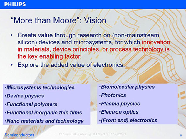
Original PowerPoint slide from 2003
Then, the entire semiconductor industry embraced the catchphrase. The International Technology Roadmap for Semiconductors (ITRS), in which organizations and experts across the globe work together to align on roadmaps for semiconductors and systems, embraced ‘More than Moore’ in a 2005 whitepaper (that is still available online) calling for a broader view on the roadmap of semiconductor technology than only trying to double every two years:
The industry is now faced with the increasing importance of a new trend, “More than Moore” (MtM), where added value to devices is provided by incorporating functionalities that do not necessarily scale according to “Moore’s Law“.
All the conditions were there for MEMS to flourish
With Philips leadership support, European investments and global industry alignment, all the conditions were there for MEMS to flourish: “In the first years, we did a lot of projects for mobile phone manufacturers, but also for NXP after the spin-off in 2006. The MEMS Foundry was a place where researchers were allowed to work on new devices.”
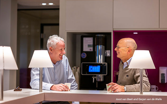
Over the years, the focus gradually shifted, says Joost van Beek, Manager Process Development & Integration: “Initially, the cleanroom was only used by and for Philips. In the early years, many researchers worked on MEMS projects. Later, we noticed that the added value of our foundry is not only in research, but rather being a production facility for MEMS. There are many fabs where you can do research on devices. In contrast, manufacturing facilities for MEMS devices are much scarcer, especially since more and more MEMS applications find their way to the market.
We still develop prototypes, but the focus of the MEMS Foundry is on volume manufacturing. That is how we have been able to develop to an industrial foundry with an experienced staff. Together, we can support customers in developing and industrializing innovative MEMS designs into a high quality manufacturing process. And we can produce those products in high volume.”
“Together, we can support customers in developing and industrializing innovative MEMS designs into a high quality manufacturing process. And we can produce those products in high volume.”
Joost van Beek, Manager Process Development & Integration
Over the years, more and more external customers found their way to the MEMS Foundry, to mature their manufacturing process and get it released for volume production. The products being manufactured cover a wide range of applications; from BioMEMS to CMUT and photonics. Joost: “One nice example is that our work has been pivotal in the development of the EUV stepper of a lithography equipment manufacturer. In our MEMS Foundry, we develop and produce large area membranes that are as thin as 10 nanometer, which are used in lithography equipment to protect the mask and wafer against dust particles.”
Gerjan: “I think it is safe to say that it has been pivotal to many innovations, both for external customers and for Philips. Looking back, the idea that there is ‘More than Moore’ was exactly the right message that sparked a sequence of events that accumulated to the MEMS Foundry as it stands today.”
If you want to learn more or discuss how we can help to realize your MEMS innovation, don’t hesitate to contact us.