
Thin film processing
Your benefit
You are looking for one or more thin film processing steps, to complement your own process capabilities. You will benefit from our rich expertise and comprehensive thin film tool kit.
We deliver
We deliver enriched substrates, involving a single layer or a more complex and patterned stack of layers. This can be in single units or volumes up to thousands of substrates per year.
Our approach
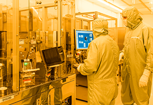
Employing our state-of-the-art tools, our ability to use a wide variety of materials (Ag to Zn, dielectrics, polymers) and substrates (Si, III/V, glass, ceramic; square & round, up to 8”), we manufacture according to your requirements.
Methodologies
- Project management
- Statistical process control (SPC)
- Quality systems ISO 9001, 13485
- DfX, design for excellence
- Cpk analysis, yield improvement

Check out our related services
When you need a custom MEMS device for your system, you can rely on our experts. Their expertise is to really understand your requirements, to show feasibility and proof of concept, develop the product and required process in a stage-gated manner and reproduce reliably & controlled.
We have over 30 years of experience in prototyping & assembly in our Micro Devices Facility called ‘Greenhouse’. Therefore, integral coupling with supply chain and manufacturing activities is assured.