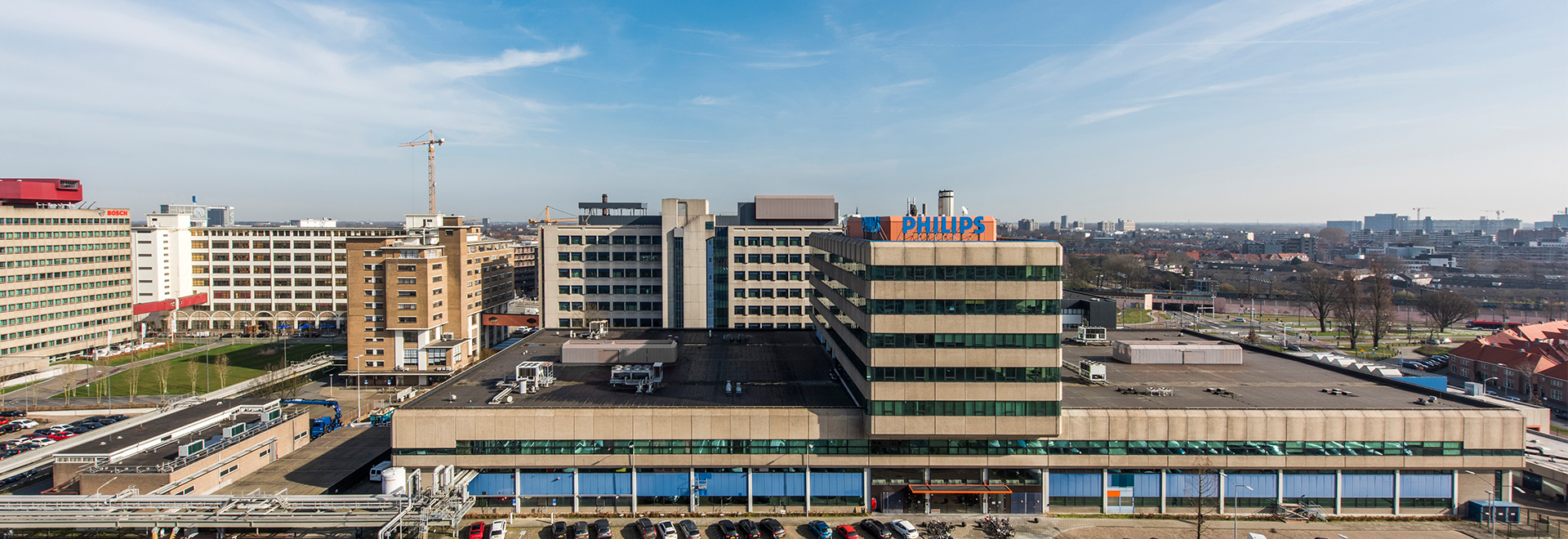
Photonics development and industrialization services
Photonics and optoelectronics are exciting areas to work in. But how do you successfully cross the Valley of Death, where most working prototypes die due to shortfalls in testing, validation and industrialization processes?
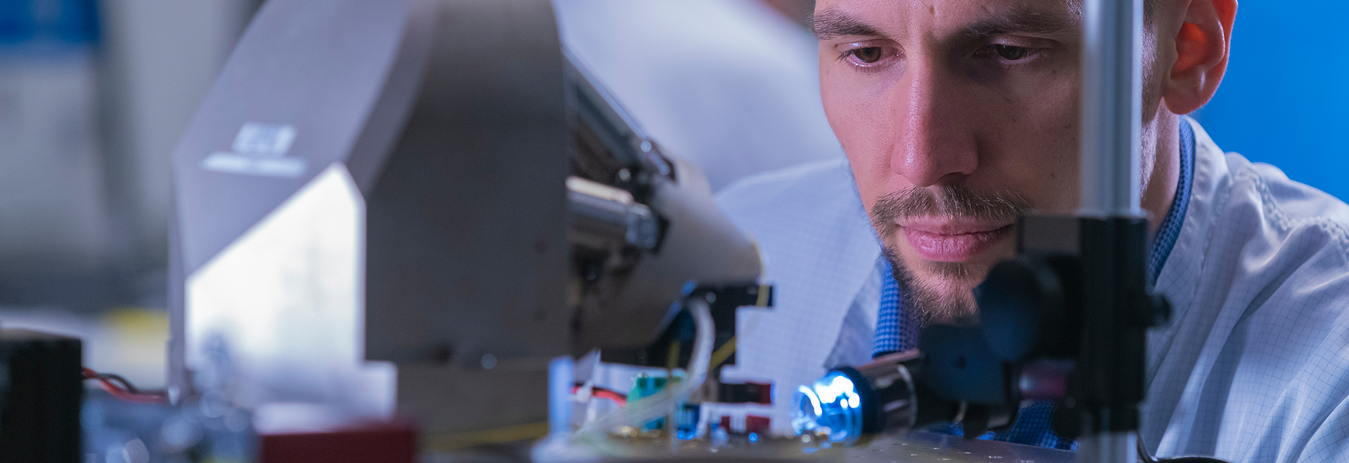
Innovation Engineering can help by expanding your reach. Our broad experience across industries in large-scale development and manufacturing is supported by state-of-the-art testing and cleanroom facilities. We have the expertise in house to shorten your photonics development time and help you achieve consistent products at volume scale.
What can we do for Photonics?
Recent developments allow us to shrink complex photonic circuits so they can be made on a chip or other substrate at the sub-millimeter level. Our unique expertise in electronics development and manufacturing helps you reliably and expertly integrate and scale up cutting edge photonic devices to manufacturing.
What is photonics?
Photonics is a technology used to generate, process and detect light that is widely used in telecommunication, manufacturing and sensing applications. Typical photonic systems include lasers, lenses, optical fibers, detectors, and more.
Direct contact
Elena Beletkaia
Business Development Manager

How to avoid common pitfalls in Photonics
Take an integrated approach to photonic integration
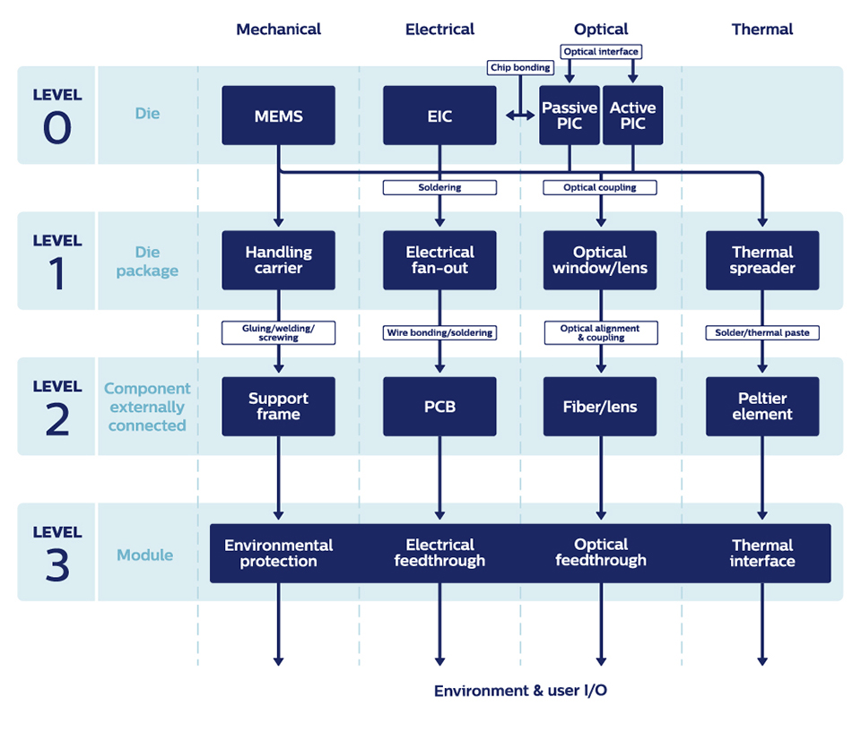
One thing we have learned about photonic assembly is that it’s never about photonic assembly alone. Besides the optical interface, the product usually has electrical, mechanical and thermal interfaces.
In addition, an electro-optical system often has to meet specific cleanliness requirements for lenses and ambient temperature requirements, so standard interconnect solutions cannot always be used. This is where our 30+ years of experience in the electronics industry makes a difference.
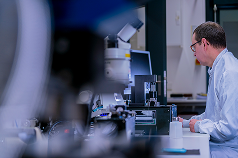
Our experienced staff operates a fully equipped micro assembly facility ready to address even your most challenging interconnection issues.
Save time and money by leveraging a mature manufacturing and assembly process
Another important aspect when developing a photonics device is how to bring it to market quickly and efficiently. Doing this without having a mature manufacturing and assembly process in place can slow down your production ramp-up and lower your production yields, which can result in unexpected costs and delivery issues.
To prevent this, we use standard industrial equipment during the development phases, rather than laboratory equipment. This enables us to make suggestions to the product while it is in the concept phase that will make it more manufacturing ready and prevent costly product changes, at a time when you want to focus on the market introduction.
By doing your product and assembly process at the same time, we can help you save significant time and money on your product introduction.
Our packaging and assembly expertise
Micro-assembly for optical modules
Our cleanroom is well equipped to help you overcome the assembly challenges involved with novel photonic or optical modules. These include:
- Alignment – highly accurate alignment at the nanometer level of passive and/or active elements is required to ensure proper functionality
- Placement and assembly – apart from accurate alignment, a reliable fixation method is also required to keep the elements aligned
- Low contamination connection – to maintain a high lifetime for the coupling and device
- Handling – photonic devices are often more fragile than electronic devices, containing glass fibers instead of copper wires, full glass components and even InP wafers, meaning they are more fragile than silicon wafers
- Automation – manual assembly is often difficult and complicated, especially for more complicated systems, where beam quality and other technical aspects need to be considered in addition to the coupling levels
- Multiple inputs/outputs – an additional challenge is providing multiple inputs/outputs for light paths

Micro-assembly for novel photonic devices
Our high-precision electronic and micro-assembly facilities have the right capabilities and a broad range of state-of-the-art industrial production equipment to assemble opto-electronic devices at industrial volume that meet high quality standards.
Using industry-standard tools and machines for novel and difficult applications allows us to lower the final costs and makes it easier to transfer the process to other manufacturing locations if desired.
For very specific high-tech equipment, we have the resources to invest in specialized tools and spread the costs over different projects to limit the upfront costs for start-ups.
Micro-assembly for photonic applications

- Electronics – chip assembly and PCBA processing. Unique expertise in integrating photonics and electronics. This includes dense wire-bonding at the submillimeter level and solder bumping that meets low temperature requirements and avoids contaminating optical surfaces
- Thermal interfaces – we can help you achieve a reliable thermal interface through industrial standard pick & place equipment that provides extensive thermal modeling to meet high thermal output, thermal stability and/or thermal expansion specifications
- Mechanical solutions – we offer a wide variety of soldering and gluing solutions to provide high precision alignment with sub-millimeter tolerance for different materials
- Material handling – thin-die, film frame carrier, tape & reel, waffle pack, gel pack, component placement
- Substrates – flex, flex-to-rigid, laminate, ceramics, lead frame, FR4, Rogers, BT, hybrids (wave guide), heatsinks
- Alignment – fiber alignment, lens alignment, active alignment, lens arrays
- Packaging – glob-top, underfill, conformal and parylene coating, dam&fill
- Die bonding techniques – thermo-compression, lead-free soldering, Au-Sn soldering, low melting SnIn/SnBi soldering, Ag-sintering, conductive and nonconductive adhesives and films (ICA, ACA, ACF, DAF), UV adhesive bonding, optical clear adhesive (OCA)
- Interconnect – wire bonding Au, Al, reflow soldering (vacuum, nitrogen, formic acid), fine-pitch flip-chip and Cu-pillar, stud-bumping (SBB), ball placement
Flex-to-rigid (F2R) for Photonics
In photonics, F2R has the potential to solve micro-assembly or complex geometrical challenges of the optical systems.

Photonics services from prototyping to volume production
- Prototyping
- Design for manufacturing, based on standard industrial equipment, Six Sigma manufacturing principles, risk management and an FMEA process
- Process development
- Ramp-up, series production, full traceability (ISO 13485), life cycle management
- Optional transfer to EMS