
GaN-on-Si
We offer the following services:
- Capability to process GaN-on-Si (dry etch, metallization) on 150 mm
- Development and manufacturing of process flows for devices
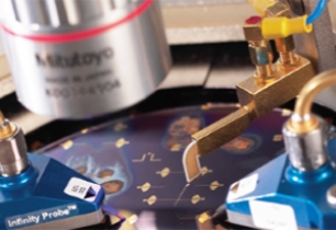
- Rapid electrical wafer characterization
- Process development, manufacturing and characterization of test structures, and passive and active devices for high-voltage and RF-power applications
- Wafer re-shaping, including re-beveling
- Development of die micro-assembly solutions
These services are on 6” wafers (max), typically provided by the customer.
Customer benefits are:
- Independent and fast electrical monitoring of EPI quality
- Electrical SPC for in-house processes
- High-quality, IP-safe source for customized active devices
- Flexibility to optimize processes to meet customer-specific device performance requirement
Check out our other MEMS applications
MEMS applications are many. Organ-on-a-chip for example, where a human organ is reproduced in its most elementary form: microelectromechanical systems device. Several applications stand out, because of their promise and our capabilities.
Relevant for you: MEMS & Micro Devices 

Sustainable competitive advantage through custom MEMS devices. Check out our services in the MEMS & Micro Devices key area of expertise.